Introduction
The KuupKulgur project researches navigation automation. To accelerate development, NVIDIA Jetson modules are used to process camera and sensor feeds. The Jetson is directly attached to the rover and commands the vehicle's movements. NVIDIA is moving toward space-oriented computing, and the lunar rover requires an intermediate transition to continue further development.
Currently, a commercially available NVIDIA Jetson development kit is being used, but the main carrier board needs to be specifically interfaced with the rover. To fit the new carrier board inside the rover, the system was split into two parts; the main carrier board, which includes essential interfaces and components for the rover, and a peripheral debug board that breaks out additional interfaces.

.png)
.png)
PCB design using KiCad
NVIDIA has provided PCB design recommendations and references to help engineers produce Jetson products for high-performance applications.
The schematics were created for the main carrier board, and the peripheral debug board. To provide a better overview, a hierarchical block system with inherited signals was used. Power signals were not inherited because of the large number of shared power connections; instead, a separate power-tree diagram was drawn.


As usual, the first iteration is not final and full reworks are typically expected due to missing design rules, layout changes, mechanical considerations, etc. A comparison between the first and final versions is shown below.
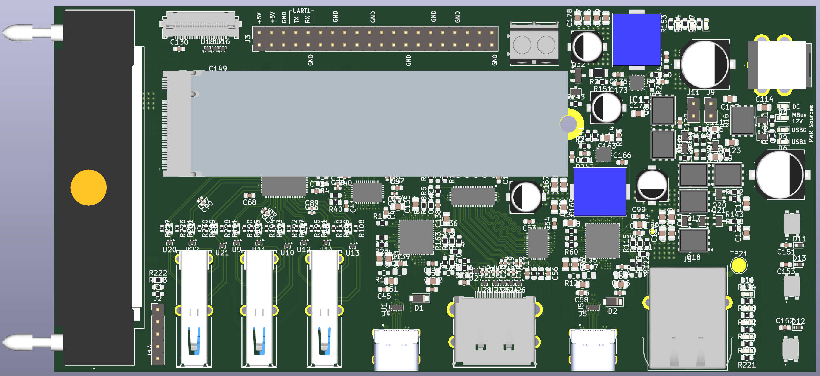
The main carrier board is the most critical, with most component locations already known; routing should be optimized to conserve the limited PCB space. The peripheral board will be designed based on the main carrier board, with the extension connector header pinout determined; peripheral components can be relocated as needed to optimize routing.
An 8-layer PCB design was implemented to accommodate the complex routing requirements and ensure signal integrity.
Main Carrier Board routing changes
Slide left or right to see the transformation from my initial ideas a years ago to the finished product of today.


Peripheral Debug Board component placement changes
Slide left or right to see the transformation from my initial ideas a years ago to the finished product of today.

Milestones & Breakthroughs
As the project design was finalized, a series of milestones and breakthroughs were achieved.

PCBs Ordered and Received
Two 8-layer PCBs were ordered from Aisler, a European manufacturer specializing in prototype PCBs.

Soldering
Additional stencils were ordered to facilitate manual application of solder paste. After applying the paste, components were placed and reflowed in a soldering oven. Connectors that cannot withstand lead-free reflow temperatures were soldered by hand.


Visual and X-Ray inspection
Soldered components were inspected visually and with X-ray imaging to ensure proper connections and identify hidden defects. X-ray imaging was needed to inspect areas under components without directly accessible pads. When issues were found, they were fixed by hand.

Solder conductivity checking
Visual inspection helps determine if solder joints have reflowed and if short circuits exist, but it can be hard to detect discontinuities. Trace resistance measurements were used to verify solder-joint integrity and soldered areas were reflowed or repaired where necessary.
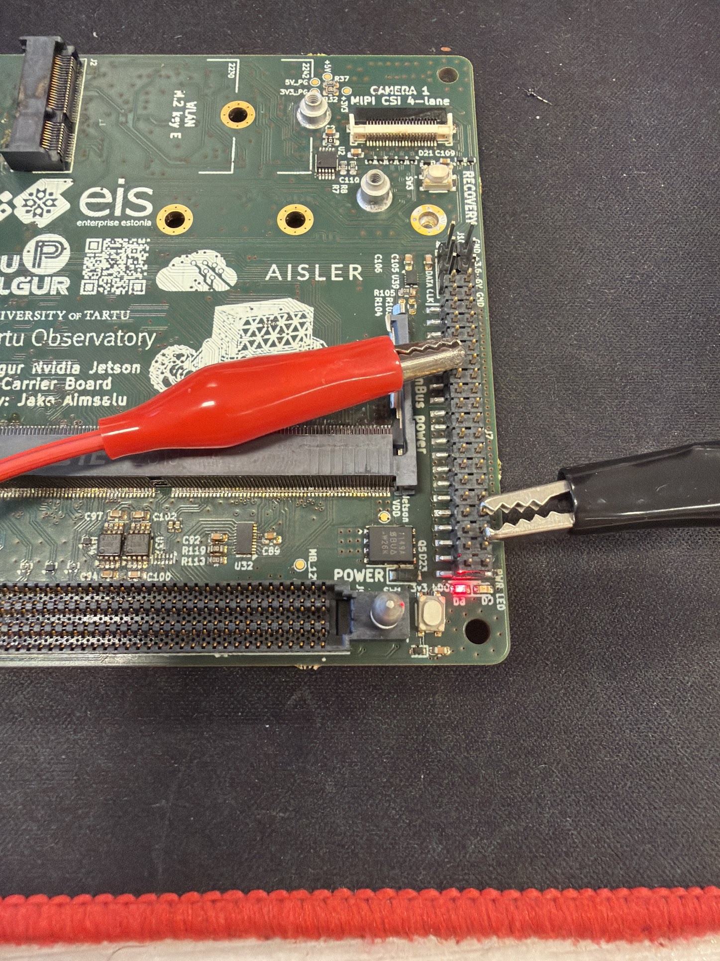
First Power-Up
The solder joints were validated to ensure proper power delivery. Power was applied with caution: using a laboratory power supply, voltage and current limits were set to mitigate potential failures.

Power-up sequence
The Power Control Module, based on an ATtiny microcontroller, was programmed to manage safe power-up and power-down procedures.
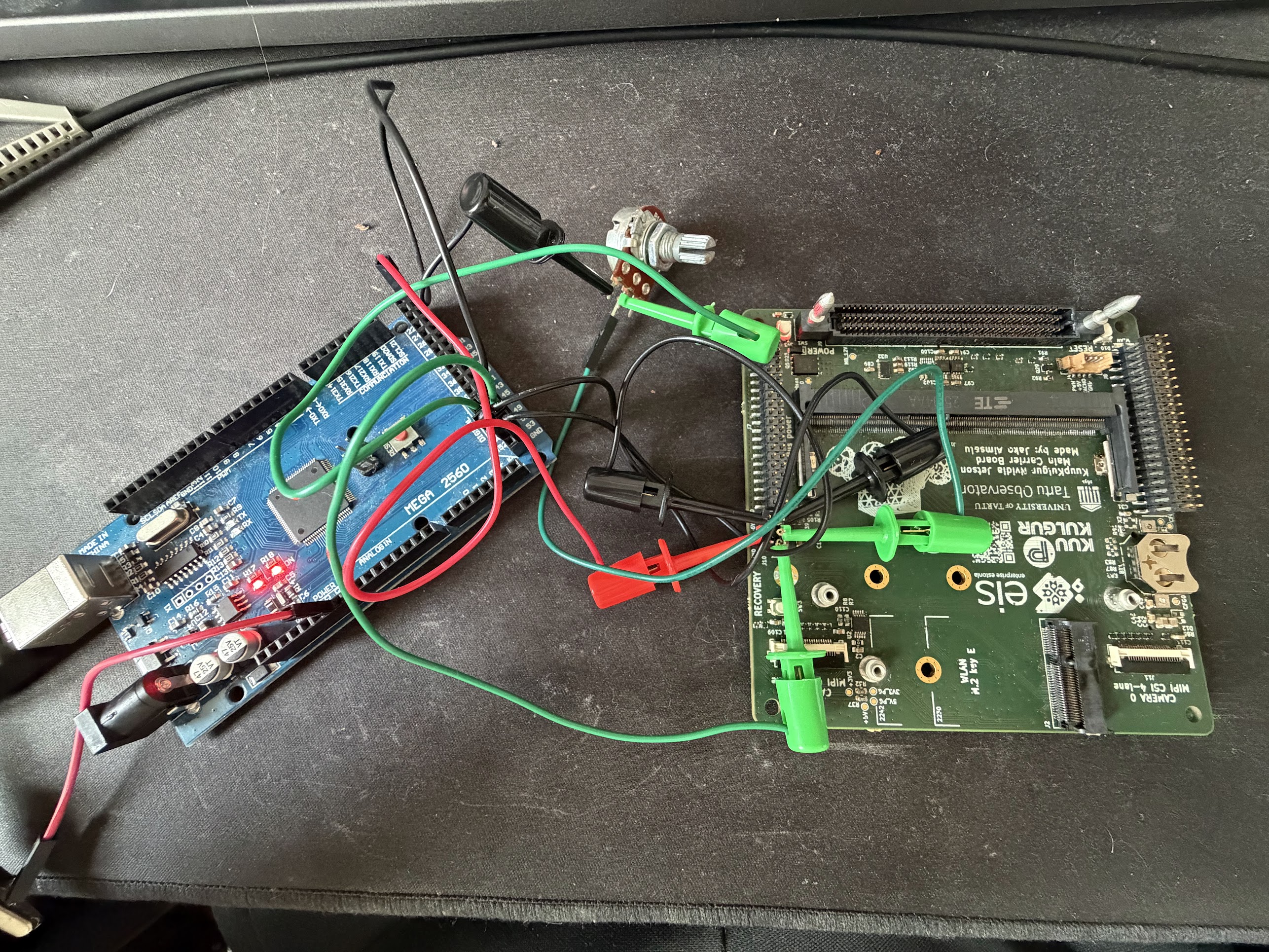

Debugging programming issues of the Power Control Module
The Power Control Module was programmed using an Arduino Mega. The protective voltage level translators were removed to decrease the noisiness in data lines.

Validating power-up sequence
Before inserting sensitive Jetson modules, voltage levels and sequencing were validated. Some voltage source selections failed due to mixed transistor pinouts and incorrect voltage ratings.


Connecting the Jetson Module
Voltage ratings and sequencing were confirmed. The Jetson Orin module was attached along with an NVMe SSD. The board was successfully powered up and recognized by the host PC for operating system installation.
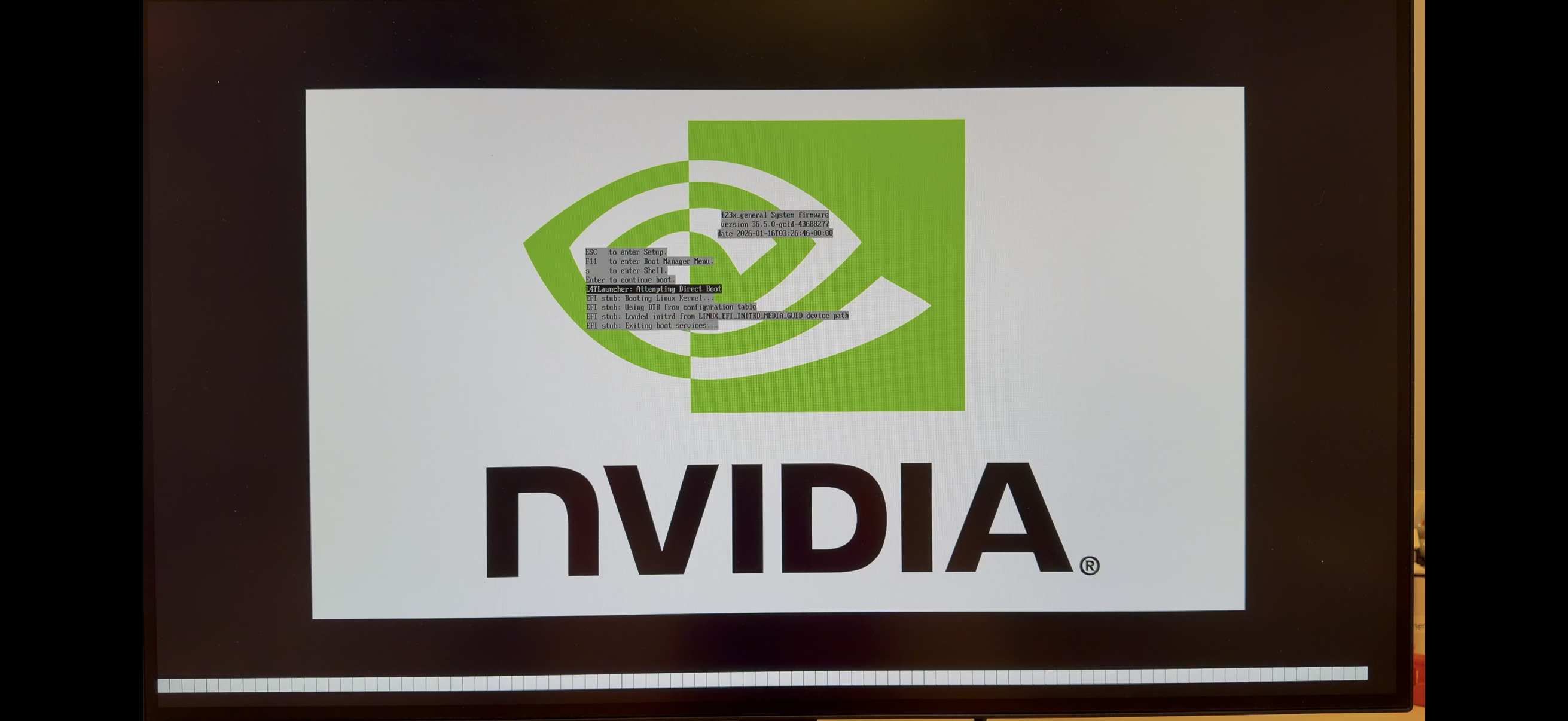
Jetson bootup
The operating system was successfully flashed. On the first boot-up, the NVIDIA logo appeared on the monitor. The hardware has now been validated and is ready for further software-related testing.
International project showcase
During Winter Satellite Workshop as Finland, Espoo, a presentation was given on the progress of NVIDIA Jetson carrier board development.
